薄膜晶体管和超大规模集成电路:竞争与合作
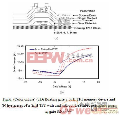
– Nonvolatile a-Si:H TFT memories. Flash memories made from poly-Si TFTs with ONO or floating-gate dielectric structures have been reported in the literature. 19–21) However, memories made from a-Si:H TFTs are rarely reported. Recently, the floating gate a-Si:H TFT has been fabricated into nonvolatile memories on a glass substrate at ≤300 oC, as shown in Fig. 6(a).22) It has a much larger hysteresis in transfer characteristics than the conventional a-Si:H TFT, as shown in Fig. 6(b).23) Memory capacitors based on the similar structure have also been demonstrated. 24) The ability of including low-temperature prepared memories to the logic circuit is desirable for both TFT circuits and ULSICs.
These recent developments raised the question on whether TFT and ULSIC will become competitive or complimentary technologies in the future.
2. Comparison of Devices, Materials, and Fabrication Processes
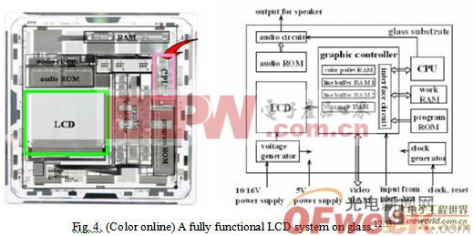
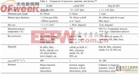
In order to compare TFT and ULSIC technologies, their basic material, process, and device properties need to be studied. Table I lists some important properties.25) These properties are closely related to product performance. For example, since the early development stage, the TFT application was focused on LCD pixel driving. The low temperature glass was the substrate of choice. Therefore, the fabrication process has to satisfy requirements of 1) largearea substrates, 2) low temperatures, and 3) high throughputs. Although most of the TFT fabrication processes were originated from ULSIC processes, there are many unique problems that cannot be solved directly from existing knowledge. New phenomena and theories have been developed during the developing of the large-area, lowtemperature TFT production process. Since some of the TFT material and process requirements are more stringent than those of the ULSIC, these new results can greatly benefit the future large wafer ULSIC process development. The following are some examples:
2.1 Large-area PECVD thin films
Plasma-enhanced chemical vapor deposition (PECVD) is the dominant thin film deposition method for a-Si:H, nþ, and SiNx layers. The availability of the doped PECVD a-Si:H film is critical to the successful demonstration of the first a-Si:H TFT.26) During the large-area PECVD SiNx study, a generalized relationship that correlated the plasma power to deposition rate, uniformity, refractive index, stress, and plasma phase particle generation has been developed.27–29) TFT characteristics, e.g., threshold voltage, are correlated to SiNx gate dielectric properties, e.g., refractive index.30) The PECVD a-Si:H deposition condition can affect the interface composition of the underneath SiNx gate dielectric through the hydrogen etching mechanism.31) The damaged interface has a large interface density of states, which lowers the threshold voltage and the field effect mobility. The hydrogen etching mechanism also plays an important role in the microcrystalline (mc) phase formation in mc-Si:H.32) The simultaneous deposition-and-etching mechanism in PECVD is critical to inter-layer dielectric, passivation, etc., which are common in ULSICs.

加入微信
获取电子行业最新资讯
搜索微信公众号:EEPW
或用微信扫描左侧二维码