薄膜晶体管和超大规模集成电路:竞争与合作
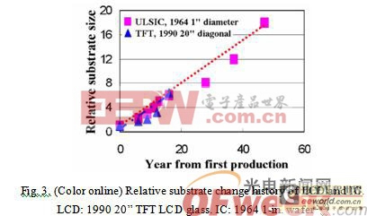
The substrate size directly influences the production throughput and therefore, the cost. Figure 3 shows changes of the relative substrate size of the TFT glass plate and the ULSIC wafer vs the production year. The rectangular glass with a diagonal size of about
TFT and ULSIC are silicon based mass production technologies. There are many efforts in preparing TFTs using non-silicon semiconductors. CdSe TFTs have been popular before 1980. Recently, organic and ZnO TFTs have made major progresses.9,10) The former has the potential of being fabricated without using the vacuum technology. The latter can be prepared by sputtering. These TFTs can be made into various chemical, photonic, and electrical sensors.11) Their low process temperature is also attractive for flexible displays. However, compared with a-Si:H and polycrystalline silicon (poly-Si) TFTs, they are in the development stage and need time to find proper markets.
Although a-Si:H and poly-Si TFTs have been successfully used as the pixel driving device in LCDs, it has been a long term goal for researchers to fabricate complicate circuits or novel products with this technology. The major advantage, which is also the biggest challenge, of the TFT technology
is its capability of achieving high performance devices on substrates with low glass transition temperatures, such as glass or plastics. Recently, there are some new developments in this area, for example:
– Complete display system on glass. A complete LCD system, which includes a 2.2-in. LCD, central processing unit (CPU), read-only memory (ROM), random access memory (RAM), graphic controller, audio circuit, etc. on a 5-in. glass, has been demonstrated, as shown in Figs. 4(a) and 4(b).12,13) Circuits with 11 MHz operation frequency composed of n- and p-type poly-Si TFTs were fabricated by a solid phase crystallization method.13) This is a proof of the feasibility of fabricating of a multi-functional system on a commercial glass.
– Panel size drivers. Two types of panel size drivers have been fabricated based on poly-Si TFTs. The first type is the integrated driver which is fabricated during the construction of the back panel TFT array. This type of plate has been demonstrated with an additional ambient light sensor system constructed.13) The second type is the independent row or column driver, as shown in Fig. 5, which is fabricated separate from the back plate TFT array.14) This kind of driver can be used to drive existing a-Si:H or poly-Si TFT arrays. Each display requires only two pieces of drivers, i.e., one for gate and one for column. Therefore, one piece of the panel size driver can replace several pieces of IC driver chips. By integrating the peripheral driver ICs with the TFT fabrication process, the TFT business (at least poly-Si TFT LCDs) becomes more independent to the ULSIC because of no necessity of outsourcing the driver ICs.15)

加入微信
获取电子行业最新资讯
搜索微信公众号:EEPW
或用微信扫描左侧二维码