使用宽带电压和电流反馈运算放大器时的应用基础
(Click to Enlarge Image)
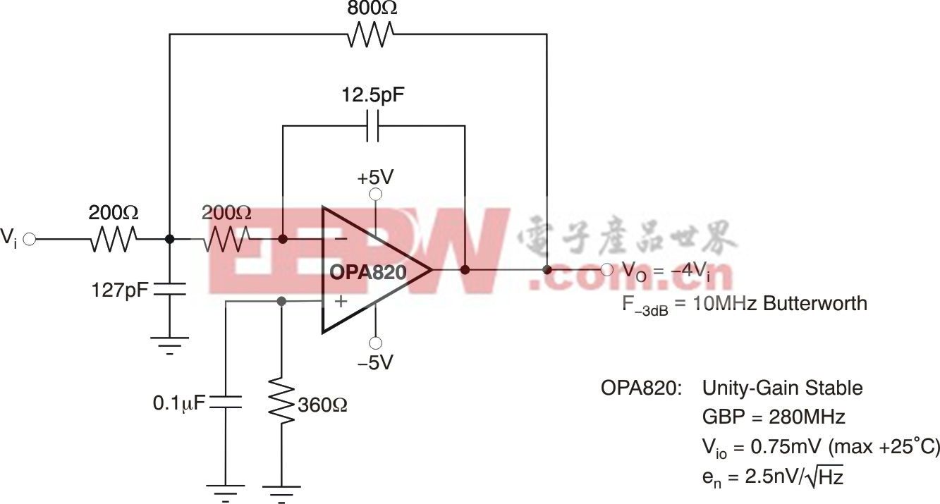
Figure 8. Example MFB filter using the OPA820.
Since the local feedback capacitor shorts out at higher frequencies, this circuit normally needs to use a unity gain stable VFB. (Reference 4suggests a path to improved phase margin in this circuit using non-unity gain stable amplifiers.) One of the advantages of the MFB design is improved stopband rejection (over the Sallen-Key filter), and very good filter accuracy versus finite amplifier gain bandwidth product. This filter tends to achieve a slightly lower Q than that targeted as the Ω0moves closer to the amplifier GBP.
(Click to Enlarge Image)
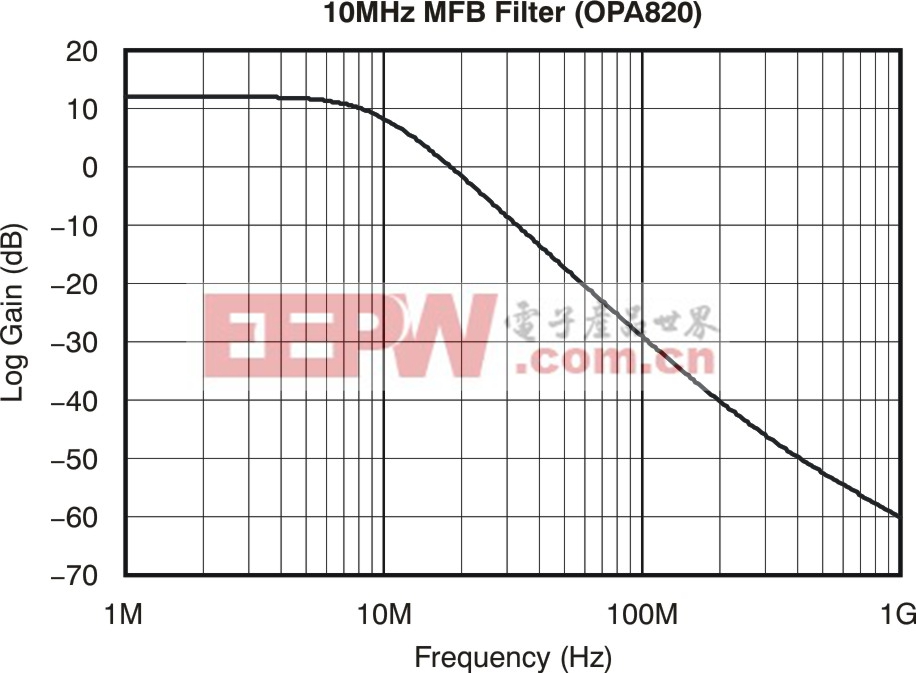
Figure 9. Simulated 10 MHz Butterworth filter of Figure 8.
C. Circuits with simple feedback poles implemented as an RC in the feedback network. Designers often implement a low-pass pole in this fashion. Since the feedback impedance is now a parallel RC network, this circuit must be implemented with a VFB, and preferably a unity-gain stable VFB. This type of simple filtering works best for inverting signal paths. In that case, the input signal sees the gain resistor as an input impedance that converts the signal to a current into the inverting node. From there, it continues into the feedback impedance to set the gain to the output.
This type of pole implemented for a noninverting configuration has a pole/zero pair because the gain transitions from a DC value set by the resistors to unity gain as the feedback capacitor shorts out at higher frequencies. Therefore, this circuit drops to unity gain if implemented as a non-inverting stage. In the inverting configuration, the gain continues down with a one pole response. It is important to notice that a unity-gain stable amplifier would be preferred because the noise gain drops to unity for either the inverting or non-inverting application.
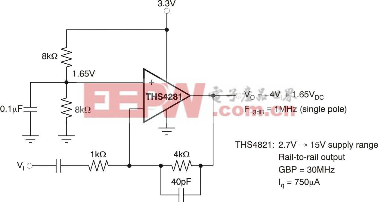
Figure 10shows an example using the THS4281 (a low-power, rail-to-rail output VFB) in the inverting configuration. In this example, the signal path was AC-coupled through a blocking capacitor. This allowed the non-inverting bias voltage to be set to mid-supply and then have a DC gain of one to the output. Because the THS4281 includes the negative rail on the input, an alternative DC-coupled design is possible by changing the lower 8 kΩ resistor on the non-inverting input to 889 Ω and removing the input blocking capacitor.
This AC-coupled design allows a direct comparison of this circuit to a low-power CFB that does not have an input range extending to ground. That device, the OPA684, also uses less than 2 mA supply current and gives greater than 100 MHz bandwidth in most applications.Figure 11compares the simulated response of this 1 MHz one pole rolloff circuit of Figure 10, using both the THS4281 and the OPA684 (where the OPA684 would use a single +5 V supply). Both parts give the expected one pole rolloff, but the OPA684 shows a very anomalous response at higher frequencies indicative of probable oscillations.
(Click to Enlarge Image)

加入微信
获取电子行业最新资讯
搜索微信公众号:EEPW
或用微信扫描左侧二维码