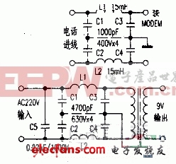
MAX4885AE应用电路图
MAX4885AE应用电路图
The MAX4885AE integrates high-bandwidth analog switches, level-translating buffers, and level-translating FET switches to implement a complete 2:1 multiplexer for VGA signals. The device provides three very high-frequency 900MHz (typ) SPDT switches for RGB signals, two low-frequency clamping switches for the DDC signals, a pair of level-translating buffers for the H and V signals and integrated extended ESD protection.Horizontal and vertical synchronization (H_/V_) inputs feature level-shifting buffers to support low-voltage controllers and standard 5V-TTL-compatible monitors, meeting the VESA requirement. Display Data Channel (DDC), consisting of SDA_ and SCL_, are FET switches that protect the low-voltage VGA source from potential damage from high-voltage presence on the monitor while reducing capacitive load.All seven output terminals of the MAX4885AE feature high-ESD protection to ±15kV Human Body Model (HBM) (see the Pin Description in the full data sheet). All other pins are protected to ±2kV Human Body Model (HBM).The MAX4885AE is specified over the extended -40°C to +85°C temperature range, and is available in a space-saving, 28-pin, 4mm × 4mm TQFN package.

典型工作电路
关键词: 电子电路图,MAX488

加入微信
获取电子行业最新资讯
搜索微信公众号:EEPW
或用微信扫描左侧二维码